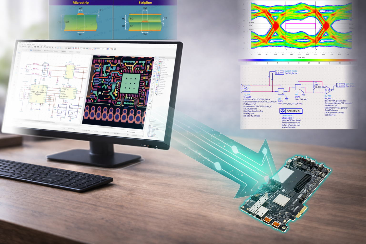
This entry showcases a selection of high-complexity hardware solutions designed for industrial-grade performance. Featuring the SLB500A and SLB400A platforms, these designs demonstrate our expertise in multi-layer stack-up optimization and comprehensive system-level architecture. Each board is engineered to meet rigorous standards, incorporating advanced thermal management and precision signal routing to ensure peak reliability in demanding digital-analog environments. Explore the detailed specifications below to see how these designs can be integrated into your next project or customized for specific industrial requirements.
SLB-500A
The SL500A board is built around a Kintex-7 FPGA, which serves as its core processing element. It features high-sampling-rate analog and digital I/O interfaces, making it well suited for medium- to high-speed digital signal processing (DSP) applications.
Designed to balance performance and cost, the SLB500A provides versatile processing capabilities while maintaining signal integrity for demanding data-acquisition tasks.
Key Features
Cost-efficient Kintex-7 FPGA offering versatile and high-performance processing
Five dual-channel ADCs, each operating at 125 MSPS
Independent low-jitter input sampling clock for optimal ADC performance
16 differential I/O channels, supporting data rates up to 400 Mbps per channel
The SL400A board is built around a Spartan-6 FPGA, which serves as its core processing element. It features 1 GB of DDR2 memory, providing high-speed volatile storage, along with a wide range of analog and digital I/O interfaces. This makes the board well suited for low-speed digital signal processing (DSP) and embedded control applications.
Thanks to support for MicroBlaze soft-core processors on the Spartan-6 platform, the SLB400A can run an RTOS or PetaLinux, enabling flexible and portable embedded system development.
Key Features
XCS6SLX45-2FGG484 FPGA
DDR2 memory with data rates up to 800 MT/s
Two isolated RS-422 channels supporting data rates up to 16 Mbps
10 independent ADC channels, each capable of sampling up to 5 MSPS
This FIR filter FPGA Vitis HLS implementation generates an optimized DSP IP core for real-time signal processing.
Finite Impulse Response (FIR) filters are among the most widely used components in digital signal processing (DSP). They are essential in applications such as wireless communications, audio processing, radar systems, and FPGA-based real-time filtering.
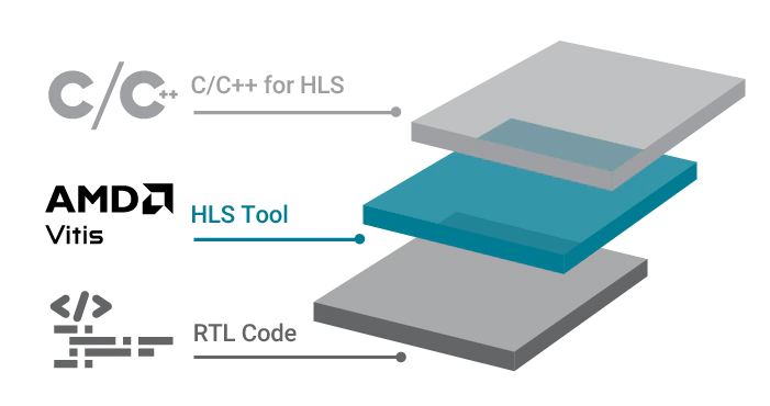
In this tutorial, we demonstrate how to implement a low-pass FIR filter on FPGA using AMD Vitis High-Level Synthesis (Vitis HLS) and deploy it as an optimized IP core.
Project Overview: FIR Filter Design Using Vitis HLS
The goal of this project is to:
Design an FIR filter in MATLAB
Implement the filter in C++
Synthesize the design into RTL using Vitis HLS
Export an FPGA-ready IP core
Verify performance through simulation and FFT analysis
This workflow is widely used in FPGA-based DSP development.
Step 1: FIR Filter Design in MATLAB
We began by designing the FIR filter using MATLAB FDATool with the following specifications:
Filter Type: Low-pass FIR filter
Cutoff Frequency: ~2 MHz
Stop-band Attenuation: ~68 dB
Coefficient Format: 16-bit signed integers
The coefficients were exported from MATLAB for use in the hardware implementation.
Step 2: FIR Filter Reference Model in C++
Next, we developed a C++ reference model to validate the filter behavior and generate golden simulation results.
The software model served as:
A functional baseline
A reference output for RTL co-simulation
A verification tool during HLS development
Step 3: Vitis HLS Workflow for FPGA Implementation
The complete Vitis HLS design flow included:
C Simulation
High-Level Synthesis (RTL generation)
RTL Co-Simulation
IP Export for FPGA integration
Vitis HLS successfully converted the FIR algorithm into a synthesizable IP core.
Step 4: Performance Optimization Techniques in Vitis HLS
In this FIR filter FPGA Vitis HLS design, loop pipelining and coefficient symmetry were applied to improve throughput.
Symmetric Coefficient Optimization
Since FIR filters often have symmetric coefficients, we leveraged symmetry to reduce the number of multiplications, cutting logic resource usage almost in half.
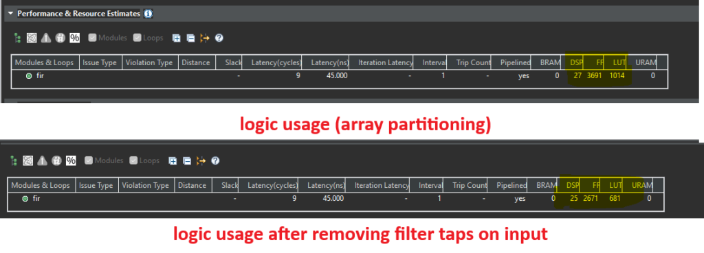
Array Partitioning
We applied the array_partition directive to enable parallel access to coefficient and delay-line arrays.
function Pipelining
Pipeline directives were added to the top function to maximize throughput.
As a result, the design achieved:
One output sample per clock cycle
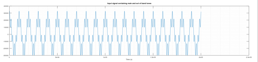
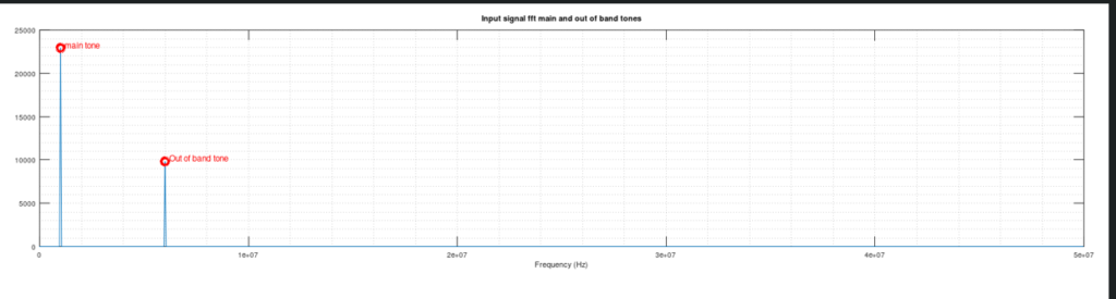
Step 5: Testbench Input Signal and FFT Analysis
To validate the FIR filter, the input signal consisted of:
A 1 MHz sinewave in the passband
A 6 MHz sinewave acting as high-frequency noise
Input Signal
FFT of Input Signal
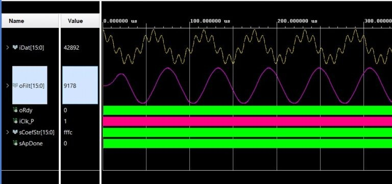
Step 6: FPGA Simulation Results Using XSim
After exporting the FIR IP core, we integrated it into a Vitis FPGA project and simulated it using XSim.
Time-Domain Output
The simulation waveform confirmed that the noise component was significantly reduced.
Frequency-Domain Output
The FFT of the output showed strong attenuation of the unwanted 6 MHz signal.
By measuring the FFT bin difference, we achieved:
~68 dB stop-band attenuation, matching the MATLAB design target.
Step 7: Simplifying and Optimizing the IP Interface
In addition to datapath optimizations, improving the IP interface structure is an important step toward building a more professional and reusable FPGA core.
In this stage, we applied optimizations to both the coefficient interface and the signal input/output ports.
Reducing Excessive Array Ports
When using array_partition, Vitis HLS may generate a separate 16-bit input port for every FIR tap. In our case, this resulted in 54 individual coefficient ports, which significantly increased interface complexity.
Since the FIR coefficients are constant, a better approach is to define them as global compile-time constants rather than passing them as input arguments. This eliminates unnecessary ports and slightly reduces overall logic utilization.
Using Modern AXI-Stream Interfaces
In many FPGA-based DSP systems, AXI-Stream interfaces are preferred because they simplify integration with the rest of the design pipeline.
To improve compatibility and system-level usability, we modified the function arguments so that Vitis HLS could automatically infer AXI-Stream input and output interfaces. This makes the generated IP core easier to connect to other processing blocks in a complete FPGA signal chain.
Frequently Asked Questions (FAQ)
What is an FIR filter in digital signal processing?
An FIR (Finite Impulse Response) filter is a digital filter commonly used in DSP because it is stable, provides linear-phase response, and is well suited for FPGA implementation.
Why use Vitis HLS for FIR filter implementation?
Vitis HLS allows designers to implement FIR filters using C/C++ instead of writing RTL manually, enabling faster development and optimized FPGA IP generation.
What optimizations improve FIR filter performance in HLS?
Common techniques include loop pipelining, array partitioning, coefficient symmetry, and resource sharing to achieve high throughput.
How do you verify FIR filter FPGA output?
Verification is typically done through C simulation, RTL co-simulation, XSim waveform analysis, and FFT-based frequency-domain validation.
Conclusion: FIR Filter IP Core Generation with Vitis HLS
This FIR filter FPGA Vitis HLS workflow demonstrates how DSP algorithms can be deployed efficiently as FPGA IP cores.